The Max
Audio Processor
Assembly
Instructions for Rev 530
Revision
date 240520
Information
contained on these web pages copyright W8KHK / N1BCG. Amateur or individual use
is encouraged.
Commercial use of
any kind is prohibited without the express written permission of the author,
Richard A. Maxwell
Content Directory
1.
General Guidelines
2.
Resources and Supporting Data
3.
Build Procedure Overview
4.
Populating the Main Processor Printed Circuit Board
5.
Initial Voltage Checks
6.
Enclosure / Chassis Preparation
7.
Front Panel Assembly Procedure
8.
Processor Board and Power Supply Integration
9.
Audio Interconnections
10.
Feature Options and Jumper Settings
11.
Illustrations – Graphics and Photographs
1: General Guidelines
The assembly process
consists of several stages; the following sequence is recommended:
1.
Main processor
board assembly (and rectifier-filter board assembly, when specified)
2.
Test and verify
functionality of power regulator and distribution circuits
3.
Chassis or
enclosure metalwork (back panel layout, drilling for connectors, controls, and
indicators)
4.
Front panel
assembly, using the “Front Panel Interface PC Board”
5.
Mount all back
panel connectors, fuse holder, power transformer (if internal supply option is
selected)
6.
Mount main
processor board and rectifier-filter board
7.
Wire audio input
and output connectors, and power leads to switch and rectifier-filter board
8.
Test and
calibrate all processor functions
9.
Connect to
microphone and transmitter, and enjoy some QSOs
An important note regarding "phantom power" for
microphones:
The input circuits do not
include any source of phantom power. If microphones which need phantom power
are contemplated, it will be necessary to use an external source between the
microphone and the processor. The rationale for this design decision focuses on
minimizing the potential for expensive microphone damage due to variations in
kit building.
NOTE: The designers of this
device assume no responsibility for microphone damage if the
builder attempts to add a phantom power source to the circuit
.2: Resources and Supporting Data
The additional files needed
to perform the assembly process are available via the RESOURCE button. They may be viewed in the main window (left
click), or downloaded (right click, then save) from the list of links on the
resource page. The following resources
are available:
Schematic diagrams:
Main Processor board,
standard version
Front Panel interface board,
1U rack version
Front Panel interface board,
mid-size desktop, style 1
Front Panel interface board,
mid-size desktop style 2
Front Panel interface board,
small desktop version
Bill of Materials and Parts List spreadsheets:
Bill of materials
Parts list in schematic
component ID sequence
Parts list grouped by
functional section of the schematic
Parts list in component value
sequence
Note: Additional graphics and photographs
illustrating the physical PC board layouts and trace paths are provided in the
2D and x-ray views toward the end of this document.
Sample Processor - Medium Desktop Style 1 with Wall
Transformer option:
Organizing Parts Inventory using the three spreadsheets
Three versions of the parts
list (identical in content, different in sequence), and a Bill of Materials,
are provided. Click the links above to access these files:
1.
Organized by
Component Value: for parts acquisition and inventory (The step-by-step assembly
instructions follow the component value sequence, as this is the most efficient
and error-free method.)
2.
In sequence by
Component Number: for careful verification of component locations on PC board (This list makes it easy to correlate proper
part value for each component number, rather than needing to refer directly to
component values on the schematic diagram sheets.)
3.
Grouped by
Function: to enable the inclusion or exclusion of processor modules
The Bill of Materials with
component values and counts will also be helpful to organize the inventory:
There will be many extra,
left-over parts when the build is completed, for three reasons:
·
Kit part counts
will be "counted high", to ensure there is no shortage when kit is
received;
·
Parts can easily
become "lost in the carpet", so extras are provided wherever
practical;
·
Some options
will require parts of different value, thus leaving extra parts out of the
build.
3: Build Procedure
Overview
The "Legends" that
identify component locations are arranged on the printed circuit board such
that they are not covered, or hidden, by the components as they are installed.
In order to avoid any confusion or ambiguity, the legends are consistently
placed either TO THE RIGHT of the component, or DIRECTLY ABOVE the component,
depending upon where space is available for the legend text. As an additional
aid in locating components by number, you may wish to either photocopy the
board silkscreen, and keep a printed copy as you assemble. Optionally, you may
be able to print an image of your board from the MAX website. In this case, be
CERTAIN that the board revision number and board date code on the printout
match the board you are building.
Diodes should be installed
before resistors, such that risk of inadvertently installing one type device in
the other type's location, is minimized.
(Simply follow the
recommended step-by-step instructions, checking off each component as it is
inserted and soldered to the main board.)
When installing resistors,
or other color-coded components, it is much easier to trace and troubleshoot
issues after assembly, if all these devices have their color code orientation
either top to bottom, or left to right. All resistors with a tan background are
carbon composition, four color bands: digit one, digit two, a multiplier, and a
tolerance band from left to right. The resistors with a blue/green background
are metal film resistors, having five color bands: digit 1, digit 2, digit 3, a
multiplier, and a tolerance band. Either type resistor may be supplied and used
anywhere in the processor with identical performance.
Inserting and Soldering Components
The easiest and quickest
(but not the best) method is to insert the device, solder both leads, then trim
the excess wire leads. A better, more professional and reliable method consists
of a few additional steps. First, insert the resistor, and solder one of the
wires. Invert the board (after soldering one wire of several resistors, if
desired) and ensure the resistor, or other device, is flush with the board
surface. Now trim both leads, solder the unsoldered lead, then go back and
reheat/resolder the first soldered lead.
This technique provides
several benefits: It ensures a neater layout, with all devices close to the
board; it avoids any risk of a cold solder joint, where the first solder
connection could be compromised if the component moves while solder is cooling;
soldering after trimming the wire ensures the solder contacts the bare wire where
it is cut, guaranteeing a no-loss contact, and last but most important, there
are no sharp points that are uncomfortable when handling the board, and the
contacts will not protrude and touch a metal enclosure if they are all trimmed
carefully before soldering.
This technique applies to
all wired components, including trim pot leads. Non-wired components, such as
Dupont or Berg pin headers, JST connectors, IC sockets should NOT be trimmed,
either before or after soldering. When installing IC sockets, first solder only
the two diagonally-opposite pins (pin 1 and 5 on an 8-pin device) then invert
the board to ensure the socket is flush with the board. If not, reheat the pin,
push the socket flush, then solder the remaining pins. For strings of Dupont or
berg header pins, solder just ONE terminal, then make sure the assembly is
flush with the board AND vertical in both planes, before soldering the
remaining pins. After all soldering is completed, solder flux may optionally be
removed with a spray or brush-on removal chemical, but this is not required for
proper device performance.
Component Legend Nomenclature
Most components are
identified by a single letter followed by a sequence number, for example R1 is
the first resistor as seen on the schematic diagram. If the parts list
indicates a suffix, such as R5A, R5B, R5C, etc. please check the optional build
instructions to determine which value to install to achieve your desired
results. Normally only one of the resistors will be used.
The processor employs extensive
power supply decoupling and filtering to provide noise and hum free operation.
Each integrated circuit will have one or more disc ceramic capacitors to bypass
each power rail. The capacitors associated with chip U11 will be identified as
C11N and C11P, which are simply the negative and positive power supply sources
for this chip. These are NOT to be confused with C11, which may or may not
exist.
The same nomenclature method
is applied to the decoupling resistors, R11N and R11p. If the chip also has one
or two electrolytic capacitors in its vicinity, those capacitors will be
identified as C11EN and C11EP. All components with no such letter suffix are
actively involved in the signal circuits and are not related to power
distribution, with the exception of components in the 3XX series, which are
parts comprising the power supply.
4: Populating the
Main Processor Printed Circuit Board
The documented component
installation sequence that follows is designed to make it easy to access all
components in the allotted space, without complications which would result if
trying to install very small components after larger, taller components are on
the board. For this reason, it is
suggested that the builder follow this proposed assembly sequence.
Before starting
assembly, please be sure to review the “Inserting and Soldering Components”
paragraph (above), to achieve the highest possible build and operational
quality.
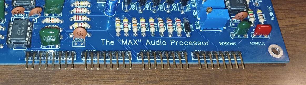
Board Interconnect Header Installation
Prior to any other
components, it is preferable to attach the 36 pin Berg Male Pin Header, used to
interconnect the main processor board with the front panel interface printed
circuit board, which will be assembled later.
It is very important that this connector be installed such that the
black insulation plastic is in flush contact with the board surface, and that
the right-angle pins protrude forward, aligned perfectly parallel to the
surface of the main board. This will
enable the two boards to interconnect reliably and without difficulty.
Prepare the 32-pin male
right angle connector as follows:
The connector actually
consists of four groups of 8 pins, but the plastic insulator is unbroken,
occupying the space of 35 pins. In order
to configure it properly, carefully pull and remove pins in locations 9, 18, and
27, leaving four groups of exactly eight pins each. Carefully cut the header plastic at the
center of pin location number 36, making sure that the plastic holding the last
pin in group four (pin location 35) is not compromised. Once the header is prepared, insert it into a
40-pin female Berg receptacle, to maintain pin alignment and protect the pins
from being bent during the remaining assembly procedure.
Extremely Critical Instruction:
The orientation of the
right-angle male pin connector differs, depending upon whether it will be used
in a desktop or a 1U Rack enclosure. If
you are assembling the desktop version of the processor, the 36-pin connector
will be attached to the top (silkscreen side) of the PC board. If you are assembling the 1U Rack version,
the connector MUST be installed on the bottom (solder, not silkscreen) side of
the PC board.
Position the prepared header
on the main board, with the pins facing forward (away from the center of the
board) and carefully solder one pin on each end of the board. Inspect thoroughly to be sure the alignment
is proper, with the surface of the pins parallel to the main board, and the
bottom of the plastic insulator in flush contact with the board surface. If necessary, reheat one or both solder
connections and make the required adjustments.
When the correct alignment
is confirmed, solder one of the pins in the center of each group of eight pins,
and re-inspect for alignment. If all is
well, solder all the remaining pins.
Sample view of interconnect pin
orientation (earlier 32-pin version shown):
Main Processor
interconnection with Front Panel Interface printed circuit board:
Diodes:
Insert and solder (seven)
glass 1N914 diodes, observing polarity band, at these locations:
[ ] D101
[ ] D102
[ ] D103
[ ] D151
[ ] D152
[ ] D153
[ ] D154
Insert and solder (thirteen)
black 1N4007 diodes, observing polarity band, at these locations:
[ ] D155
[ ] D301
[ ] D302
[ ] D303
[ ] D304
[ ] D305
[ ] D306
[ ] D307
[ ] D308
[ ] D309
[ ] D310
[ ] D311
[ ] D312
Insert and solder (four)
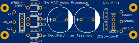
black 1N4007 diodes on the separate rectifier filter board at locations:
[ ] D1
[ ] D2
[ ] D3
[ ] D4
Resistors:
While the orientation of the
resistor has no effect on the electrical operation, it is considered preferable
to insert the device such that the color code reads from left to right or from
top to bottom, depending upon the position of the lands on the printed circuit
board.
Insert and solder (four) 10
ohm resistors (Brown, Black, Black) at the following locations:
[ ] R 121p
[ ] R 141n
[ ] R 141p
[ ] R 151p
Insert and solder (one) 33
ohm resistor (Orange, Orange, Black) at the following locations:
[ ] R 11
Insert and solder (eight) 47
ohm resistors (Yellow, Violet, Black) at the following locations:
[ ] R 189
[ ] R 190
[ ] R 209
[ ] R 210
[ ] R 061n
[ ] R 061p
[ ] R 101n
[ ] R 101p
Insert and solder (nine) 100
ohm resistors (Brown, Black, Brown) at the following locations:
[ ] R 17
[ ] R 18
[ ] R 139
[ ] R 011n
[ ] R 011p
[ ] R 012n
[ ] R 012p
[ ] R 021n
[ ] R 021p
Insert and solder (six) 470
ohm resistors (Yellow, Violet, Brown) at the following locations:
[ ] R1
[ ] R2
[ ] R 122
[ ] R 133
[ ] R 134
[ ] R 135
Insert and solder (eight) 1K
ohm resistors (Brown, Black, Red) at the following locations:
[ ] R 14
[ ] R 92
[ ] R 102
[ ] R 131
[ ] R 138
[ ] R 154
[ ] R 155
[ ] R 171
Insert and solder (three)
1.5K ohm resistors (Brown, Green, Red) at the following locations:
[ ] R 8
[ ] R 9
[ ] R 121
Insert and solder (three)
2.2K ohm resistors (Red, Red, Red) at the following locations:
[ ] R 145
[ ] R 150
[ ] R 160
Insert and solder (two) 2.7K
ohm resistors (Red, Violet, Red) at the following locations:
[ ] R 169
[ ] R 170
Optional: * On Front Panel
Interface Printed Circuit Board (for 3-position "Density" control)
Insert and solder (one) 4.7K ohm resistor
(Yellow, Violet, Red) at the following locations:
[ ] R 1
*Note: If using only a two
position "Density" switch with no center-off position, do not install
this resistor.
Continuing with the main
audio processor printed circuit board:
Insert and solder
(twenty-one) 4.7K ohm resistors (Yellow, Violet, Red) at the following
locations:
[ ] R 4
[ ] R 5
[ ] R 6
[ ] R 7
[ ] R 106
[ ] R 107
[ ] R 108
[ ] R 136
[ ] R 137
[ ] R 141
[ ] R 142
[ ] R 147
[ ] R 152
[ ] R 153
[ ] R 164
[ ] R 165
[ ] R 166
[ ] R 167
[ ] R 168
[ ] R 172
[ ] R 173
Insert and solder (one) 6.8K
ohm resistor (Blue, Gray, Red) at the following locations:
[ ] R 146
Insert and solder (forty)
10K ohm resistors (Brown, Black, Orange) at the following locations:
[ ] R 3
[ ] R 13
[ ] R 23
[ ] R 24
[ ] R 61
[ ] R 62
[ ] R 63
[ ] R 64
[ ] R 65
[ ] R 66
[ ] R 67
[ ] R 68
[ ] R 69
[ ] R 70
[ ] R 71
[ ] R 72
[ ] R 73
[ ] R 74
[ ] R 75
[ ] R 76
[ ] R 77
[ ] R 78
[ ] R 79
[ ] R 80
[ ] R 81
[ ] R 82
[ ] R 83
[ ] R 84
[ ] R 91
[ ] R 93
[ ] R 95
[ ] R 103
[ ] R 116
[ ] R 156
[ ] R 157
[ ] R 159
[ ] R 162
[ ] R 174
[ ] R 184
[ ] R 204
Insert and solder (one) 15K
ohm resistor (Brown, Green, Orange) at the following locations:
[ ] R 94
Insert and solder (thirteen)
20K ohm resistors (Red, Black, Orange) at the following locations:
[ ] R 101
[ ] R 182
[ ] R 183
[ ] R 185
[ ] R 186
[ ] R 187
[ ] R 188
[ ] R 202
[ ] R 203
[ ] R 205
[ ] R 206
[ ] R 207
[ ] R 208
Insert and solder (one) 33K
ohm resistor (Orange, Orange, Orange) at the following locations:
[ ] R 115
Insert and solder (four) 47K
ohm resistors (Yellow, Violet, Orange) at the following locations
[ ] R 15
[ ] R 109
[ ] R 132
[ ] R 158
Insert and solder (four) 100
K ohm resistors (Brown, Black, Yelllow) at the following locations:
[ ] R 85
[ ] R 144
[ ] R 151
[ ] R 163
Insert and solder (one) 470K
ohm resistor (Yellow, Violet, Yellow)
at the following locations:
[ ] R 113
Insert
and solder (four) 1 megohm resistors
(Brown, Black, Green) at the following locations:
[ ] R 111
[ ] R 112
[ ] R 114
[ ] R 161
Integrated Circuit Sockets:
Insert and solder (fifteen)
8 pin IC sockets at the following locations:
First solder the opposite
corner pins, ensure the socket is flush with the board, then solder the
remaining pins, being careful to align the index notch of the socket in the
direction matching the silk screen legend.
[ ] U 11
[ ] U 12
[ ] U 21
[ ] U 61
[ ] U 62
[ ] U 63
[ ] U 64
[ ] U 100
[ ] U 101
[ ] U 121
[ ] U 141
[ ] U 142
[ ] U 151
[ ] U 181
[ ] U 201
Insert and solder (one) 14
pin IC socket at the following location:
(Follow instructions for
alignment and orientation as done for the 8-pin sockets above)
[ ] U 152
Small Disc Capacitors:
(mylars and electrolytics
will be added later)
Insert and solder (eight) 33
pF disk capacitors at the following locations:
[ ] C 181
[ ] C 182
[ ] C 183
[ ] C 184
[ ] C 201
[ ] C 202
[ ] C 203
[ ] C 204
Insert and solder (three)
200 pF disk capacitors at the following locations:
[ ] C 5
[ ] C 6
[ ] C 7
Insert and solder (one) 470
pF disk capacitor at the following locations:
[ ] C 11
Insert and solder (four)
.001 uF disk capacitors at the following locations:
[ ] C 1
[ ] C 2
[ ] C 3
[ ] C 4
Insert and solder (six) .001
uF disk capacitors on the separate rectifier filter board at locations:
[ ] C 1
[ ] C 2
[ ] C 3
[ ] C 4
[ ] C 5
[ ] C 6
Insert and solder
(thirty-eight) .1 uF disk capacitors at the following locations:
[ ] C 131
[ ] C 132
[ ] C 154
[ ] C 156
[ ] C 306
[ ] C 307
[ ] C 312
[ ] C 313
[ ] C 101n
[ ] C 101p
[ ] C 102n
[ ] C 102p
[ ] C 11n
[ ] C 11p
[ ] C 121p
[ ] C 12n
[ ] C 12p
[ ] C 141n
[ ] C 141p
[ ] C 142n
[ ] C 142p
[ ] C 151n
[ ] C 151p
[ ] C 152p
[ ] C 181n
[ ] C 181p
[ ] C 201n
[ ] C 201p
[ ] C 21n
[ ] C 21p
[ ] C 61n
[ ] C 61p
[ ] C 62n
[ ] C 62p
[ ] C 63n
[ ] C 63p
[ ] C 64n
[ ] C 64p
Berg Header Pins:
NOTE: In place of Berg male
header pins and Dupont wires, you may optionally use the JST (Japan Solderless
Terminal) sockets and wire assemblies (may be optionally provided in the kit)
to interconnect the line input, microphone input, and line output XLR or TRS
audio connectors. These steps are
identified with three * (***) Note
also that an optional selection is required for some trim pots and headers,
depending upon whether you are building a processor with two level controls on
the front panel (STYLE 1) or four level controls (STYLE 2).
Straight Berg male headers
come in sticks of 40 pins. Cut at the notch, as needed, to install the
following length headers:
Insert and solder 3-pin Berg
male headers at the following locations:
SEE NOTE * BELOW BEFORE
PROCEEDING!
[ ] MIC *** Mic
Input
[ ] LINE *** Line
Input
[ ] R 10 * Line
Level
[ ] R 12 * Mic
Level
[ ] R 16 ** Mic
Input Gain Set
[ ] INSRT Internal
Insert for EQ or other internal option
[ ] LDR Half
Full
[ ] OUT1 *** Output
1
[ ] OUT2 *** Output
2
[ ] CMP Compressor
enable / bypass
[ ] SCAF SCAF
enable / bypass
* Note: If you wish the
front panel to be a vernier adjustment, you may install a 10K (103) trim pot at
location(s) R10 and R12, (instead of the Berg header) allowing you to preset
the maximum line and mic input level, respectively.
** Note: The MIC input, as
implemented above with a Berg header, may be jumper configured as either a line
or a mic input, setting to unity gain when configured for line input. If the
builder desires a "gain trim" function, similar to that on a typical
microphone mixing board, either a 100 ohm (101) or a 500 ohm (501) trim pot may
be installed at location R16. See
additional information in the Trim Pot section.
*** Choose either Berg male
pin headers or JST connectors at *** locations.
Insert and solder 4-pin Berg
male headers at the following locations:
[ ] Power AC
or DC In
[ ] R108 OPTIONAL: Limiter Drive 10K pot, 4.7K fixed resistor,
or jumper pin 1 to pin 4
Insert and solder 4-pin Berg
male headers on the separate rectifier/filter board at locations:
[ ] +DC G -DC
(on Rectifier Filter board) OUTPUT DC POWER TO MAIN PROCESSOR BOARD
(A flat pre-fabricated
ribbon cable will be used to interconnect the rectifier/filter board to the
main board.)
Insert and solder 6-pin Berg
male headers at the following location:
[ ] EQ1 Used
to select either main output 2 or “Insert Send” signal at OUT2 output.
If you have not already
installed the right-angle connector to the front of the board, please return to
the beginning of these instructions, and complete that step now.
[ ] Front Panel Interconnect RIGHT ANGLE Male
Connector (Instructions at beginning of document)
DO NOT INSTALL ANY BERG
HEADERS at the following locations:
These functions will be
controlled by devices on the front panel
[ ] INSW Line
Mic The input selection is
provided by the front panel mic/line switch
[ ] R 181 Output
1 Level This level will be
controlled by the front panel pot
[ ] R 201 * Output
2 Level Install pins or trim pot only
for STYLE 1, not for STYLE 2 panels.
[ ] DC1 -5
G +5 -12 G +12 (voltage test points)
Trim Pots:
*Before starting the trim
pots, see notes on the following page!
Insert and solder 100 ohm or
500-ohm trim pot in the following location:
Numbers in (parenthesis)
indicate the resistance value code printed on the trim pot
[ ] R 16 OPTIONALLY- either a 100 ohm (101) or
a 500 ohm (501) trim pot
See Note * in Berg Header
Pins section regarding gain trim pot
100
ohm (101) allows moderate setting of mic input gain trim
500
ohm (501) allows mic gain trim to be extended downward to even less gain
Insert and solder 100-ohm
trim pot (101) in the following location:
[ ] R 130 Pos
Peak Limit (initial setting will be
fully counterclockwise until clicks
Insert and solder 1000-ohm
trim pot (102) in the following location:
[ ] R 140 Neg
Peak Limit (initial setting will be
fully clockwise until clicks)
Insert and solder 10 K ohm
trim pots (103) in the following locations:
The following two * are
optional, depending upon related decision in the Berg Header Pins section
[ ] R 10 * Line
Input Preset (initial setting will be
fully clockwise until clicks)
[ ] R 12 * Mic
Input Preset (initial setting will be
fully clockwise until clicks)
[ ] R 108 Lim
Drive OPTIONAL: (initial setting will be fully clockwise
until clicks)
[ ] R 123 Bandwidth
Clock Narrow Setting
[ ] R 125 **** Bandwidth
Clock Wide Setting
[ ] R 140 Neg
Peak Limit (initial setting will be
fully clockwise until clicks)
[ ] R 201 Output
2 Level Install pins or trim pot only
for STYLE 1, not for STYLE 2 panels.
Insert and solder 20 K ohm
(203) or 25K (253) trim pots in the following location:
[ ] R 124 Bandwidth
Clock Medium Setting
* Note: If installing trim pots at these locations,
the trim pots will set the MAXIMUM LEVEL possible on the related input, making
the front panel pot function as a vernier.
Or, the front panel pot may be set at a specific location, then the R10
and R12 may be adjusted for proper input level, allowing the mic/line switch to
select either one without the need to readjust the front panel pot.
If you wish the front panel
pot to have full control, use berg pin jumpers, and a jumper may be applied
between pins 2 and 3 after assembly.
This option exposes the signals for test and diagnosis, if needed for
troubleshooting the various sections of the processor.
Another option to give the
front panel knob full control is to install the trim pots, then set them fully
clockwise until the trim pot "clicks", thus simulating the jumper
from pin 2 to 3, but also letting you revert back to option one with no
hardware change.
**** R125 sets the clock
frequency for the wide setting of the bandwidth SCAF selection. If desired, the trim pot may be set aside,
and either a Berg or JST header may be installed at the R125 location. Then a 10K knob-pot may be installed either
on the panel or at the back of the processor, and it would be wired to connect
to the header at R125. This will allow a
continuously-variable adjustment of the bandwidth when the switch is set to the
wide position. It is possible to mount
this pot at the OUTPUT 2 control location on the front panel, and in that case,
the output 2 level may be adjusted via a 10K trim pot at location R201.
Transistors:
Insert and solder (one)
2N3819 FET Transistor at the following location:
Align flat side of device
with matching silkscreen footprint
Position the device such
that 1/4" to 3/8" lead length remains between board and semiconductor
[ ] Q 101
Insert and solder (three)
2N3904 NPN Bipolar Transistors at the following locations:
Align flat side of device
with matching silkscreen footprint
Position the device such
that 1/4" to 3/8" lead length remains between board and semiconductor
[ ] Q 131
[ ] Q 132
[ ] Q 155
Insert and solder (nine)
2N3906 PNP Bipolar Transistors at the following locations:
Align flat side of device
with matching silkscreen footprint
Position the device such
that 1/4" to 3/8" lead length remains between board and semiconductor
[ ] Q 102
[ ] Q 103
[ ] Q 133
[ ] Q 134
[ ] Q 135
[ ] Q 151
[ ] Q 152
[ ] Q 153
[ ] Q 154
Mylar Capacitors:
Insert and solder (two) .001
uF mylar capacitors at the following locations:
[ ] C 121
[ ] C 144
Insert and solder (one)
.0015 uF mylar capacitor at the following locations:
[ ] C 123
Insert and solder (one)
.0022 uF mylar capacitor at the following locations:
[ ] C 94A
DO NOT INSTALL A CAPACITOR
AT C94B!
[ ] C 94B
optional - See MODS page on the Max Processor website
Insert and solder (one)
.0047 uF mylar capacitor at the following locations:
[ ] C 133
Insert and solder (two) .01
uF mylar capacitors at the following locations:
[ ] C 103
[ ] C 122
Insert and solder (one) .022
uF mylar capacitor at the following locations:
[ ] C 93A
DO NOT INSTALL A CAPACITOR
AT C93B!
[ ] C 93B
optional - See MODS page on the Max Processor website
Insert and solder (ten) .047
uF mylar capacitors at the following locations:
[ ] C 21
[ ] C 22
[ ] C 61
[ ] C 62
[ ] C 63
[ ] C 64
[ ] C 65
[ ] C 66
[ ] C 67
[ ] C 68
Insert and solder (one) .1
uF mylar capacitor at the following location:
[ ] C 91
Electrolytic Capacitors:
Observe polarity, matching
the white stripe on the negative side of the capacitor with the matching
identifier on the footprint silkscreen.
The longer wire lead is normally the positive terminal.
Insert and solder (seven)
4.7 uF electrolytic capacitors at the following locations:
[ ] C 10
[ ] C 69
[ ] C 134
[ ] C 151
[ ] C 152
[ ] C 153
[ ] C 155
Insert and solder (two) 10
uF electrolytic capacitors at the following locations:
[ ] C 142
[ ] C 143
Insert and solder (fourteen)
22 uF electrolytic capacitors at the following locations:
[ ] C 104
[ ] C 101en
[ ] C 101ep
[ ] C 11en
[ ] C 11ep
[ ] C 12en
[ ] C 12ep
[ ] C 141en
[ ] C 141ep
[ ] C 152ep
[ ] C 21en
[ ] C 21ep
[ ] C 61en
[ ] C 61ep
Insert and solder (three) 47
uF electrolytic capacitors at the following locations:
[ ] C 8
Note May be 22 uF or 47 uF
[ ] C 9
Note May be 22 uF or 47 uF
[ ] C 121ep
Note May be 22 uF or 47 uF
Insert and solder (seven)
100 uF electrolytic capacitors at the following locations:
[ ] C 105
[ ] C 303
[ ] C 304
[ ] C 308
[ ] C 309
[ ] C 310
[ ] C 311
Insert and solder (two) 3300
uF electrolytic capacitors at the following locations:
[ ] C 301
[ ] C 302
Insert and solder (two) 3300
uF electrolytic capacitors on the separate rectifier filter board at locations:
[ ] C 1
[ ] C 2
Voltage Regulators and Heat Sinks:
Voltage regulators will be
packaged in individual envelopes, and should be kept separate until ready to
install, because the legends are often very difficult to read.
A heat sink, with the sil
pad, nylon shoulder washer, and machine screw, will be attached to each
regulator before they are soldered into the following locations:
[ ] U 301 7812
[ ] U 302 7912
[ ] U 303 7805
[ ] U 304 7905
Test Voltage Regulators:
Prior to installation of the
integrated circuit devices, it is prudent to verify the proper voltage is
present on the power rail to each chip.
Voltage measurements may vary up to ¼ volt (250 millivolts) at each
location.
Connect a power source,
either the 12 volts AC between pins 1 and 2 of POWER header, Or apply + and –
unregulated DC from the Max Audio Processor Rectifier Filter board via the
four-pin prefabricated ribbon cable, to the four pins at main board header
POWER. It is NOT necessary to observe polarity
with this ribbon cable connection. (Note
that a single DC source will NOT be sufficient to test the positive and
negative regulator ouput, and the power rails to the various IC chip sockets.)
Verify the presence of -5
volts, +5 volts, -12 volts, and +12 volts at the test points on header
DC1. The points are labeled -5, G, +5,
-12, G, and +12, where G is the ground reference pin.
Verify the plus and minus
five-volt rails at the following IC pins:
+5
on SCAF U141 and 142, pin 7, on Clock U121 pin 8, and Comparator U152 pin 3
-5
on SCAF U141 and 142, pin 2
Verify the plus and minus
twelve-volt rails at the following IC pins:
-12
on Mic Preamp U12 pin 4, and +12 on pin 7
-12
on pin 4, and + 12 on pin 8 of all ten op amps:
U11, U21, U61, U62, U63, U64, U101, U102,
U151, U181, U201
Integrated Circuits:
After regulator voltage
testing is completed, and the power rail voltage at each individual IC Socket
is verified, insert the IC chips into the sockets at the following locations:
[ ] U 11 ne5532 or LF-353 or TL-082
[ ] U 12 ssm-2019
[ ] U 21 ne5532 or LF-353 or TL-082
[ ] U 61 ne5532 or LF-353 or TL-082
[ ] U 62 ne5532 or LF-353 or TL-082
[ ] U 63 ne5532 or LF-353 or TL-082
[ ] U 64 ne5532 or LF-353 or TL-082
[ ] U 101 ne5532 or LF-353 or TL-082
[ ] U 102 ne5532 or LF-353 or TL-082
[ ] U 121 ne555
[ ] U 141 max295
[ ] U 142 max295
[ ] U 151 ne5532 or LF-353 or TL-082
[ ] U 152 lm339
[ ] U 181 ne5532 or LF-353 or TL-082
[ ] U 201 ne5532 or LF-353 or TL-082
Insert and solder (fifteen)
black 1N4007 diodes, observing polarity band, at these locations:
[
] D155
[
] D301
[
] D302
[
] D303
[
] D304
[
] D305
[
] D306
[
] D307
[
] D308
[
] D309
[
] D310
[
] D311
[
] D312
[
] D313
[
] D314
6: Enclosure /
Chassis Preparation
The required metalwork
includes the layout and drilling of holes for the controls and indicators on
the front panel, holes for connectors and fuse holder on the back panel, and
mounting holes on the base of the chassis for printed circuit board attachment
and power transformer mounting. It would
be worthwhile to read through this section before starting the actual work
especially for the 1U Rack enclosure preparation.
If a desktop enclosure is
used, all holes will be drilled in the bottom half of the chassis. No holes are needed in the U-shaped top
cover. For the 1U Rack enclosure, front
panel control and indicator holes are drilled in the removable 3/16” thick
front panel, while all other holes are drilled in the base and back of the
chassis.
In all cases, the front panel
holes will be drilled for switches, control potentiometers, and LED
indicators. The silkscreened G10 glass
epoxy dress panel will be used as a drilling “template”, thus providing an easy
method to mark the center location of each required hole.
Back panel layout design is
left to the builder. Care must be taken
to ensure clearance between connectors protruding into the enclosure from the
back, to avoid conflict with components on the main circuit board, especially
the voltage regulator heat sinks. The
main board location will be defined by the interconnect pin connector that
mates with the female header at the bottom of the front panel interface PC
board, used to interconnect all LEDs, switches, and potentiometers. Review of some of the processor photos will
provide a general idea of the required layout.
When looking at the back of the enclosure, from left to right, will be
the power connector, optional fuse holder, (used only with the internal
transformer option), the output TRS or XLR connectors, space for regulator heat
sink clearance, then the line and mic input TRS or XLR connectors. For mounting of the rectifier-filter board
and power transformer, it may be prudent to wait until more of the unit is
assembled to mark and drill for these components. When laying out the desktop enclosure, more
clearance may be realized if the connectors are placed above a center line,
rather than directly centered in the available chassis space.
Install the switches
finger-tight in the panel assembly, (carefully ensuring the key notch on the
switch threaded shaft is pointing DOWN toward the bottom of the panel). Of the
eight switches, two have a center-off position, while the others only have an
up and down position. Install the center-off switches at the "OPEN DENSE
MID" density position and the "NARROW WIDE MED" bandwidth
position. The interface PCB is then placed on the switch contacts, with the
non-silkscreened side of the interface PCB facing forward toward the switches.
While putting light pressure on the board to ensure it is as close as possible
to each switch, solder only the center (common) terminal of each switch to the
interface PCB.
Front Panel Drilling Template:
When using the dress panel
as a drilling template, it is best to attach the panel temporarily to the front
of the desktop chassis, or the free-standing front panel of the 1U rack panel,
with clear transparent tape. First
attach the top and bottom, then, while ensuring the panel is perfectly aligned
both vertically and horizontally, apply a piece of tape to each end of the
panel. This ensures the panel will not
shift in any direction while marking hole locations, thus providing perfect
hole positioning.
Using a fine-point sharpie
or similar permanent marker, trace a circle around each control or indicator
hole in the dress panel. The actual
center point may then be sighted and marked, either with the dress panel in
place or after the panel is removed.
Once marked, the hole
locations should be carefully center-punched, then a pilot hole is drilled with
a small bit. This is preferable to
drilling with a larger bit, as this method retains alignment with the center
punch location. The holes are finally enlarged, to either the same size hole as
that in the dress panel or preferably slightly larger, allowing for any
possible error in either the hole location, or the possible slight misalignment
of the panel when the marking was completed.
Carefully clear any burrs on the backside of the panel with a larger
drill.
Additional notes for the 1U Rack
IMPORTANT: When removing the dress panel from the 1U
rack panel, be sure to mark the aluminum panel to indicate the front and the
top or bottom, such that proper orientation with the dress panel is maintained
through the following steps.
NOTE: When preparing the panel for the 1U Rack
enclosure, it might be prudent to leave the end holes (for the mic/line switch
on the left, and the power switch on the right) small (pilot drill size) until
the matching holes are drilled in the rack chassis mounting tabs (later in this
assembly section.)
For the 1U rack enclosure
using the Type-3 panel, the following procedure will assist in proper alignment
and assembly, while avoiding unsightly machine screw heads on the dress
panel. The rack mount chassis kit
includes an envelope labeled "panel mounting hardware". There are
four flat-head Phillips machine screws and four nuts with captive lock washers.
The four screws will be used to attach the Bud Industries aluminum panel to
their 1U rack enclosure. The flat head screw heads will be hidden behind the
glass epoxy dress panel.
The front side of the panel
must be countersunk, such that the screw heads are flush with the front
surface. A countersink bit for this purpose is available for less than $2 at
Harbor Freight, or a bit more at Lowes, Home Depot, or your local Ace Hardware.
Use a screw, placed in the hole, while boring the countersink such that the
depth may be measured to ensure the top of the screw will be flush with the
front of the panel. It must not protrude
above the panel, and it should not drop significantly below the panel surface.
Once the countersink
operation is completed, securely attach the front panel to the mounting tabs at
each side of the rack enclosure. Then drill
a hole through the front panel, through the center of each mounting tab, to
provide a mounting location for the mic/line switch on the left, and the power
switch on the right. Enlarge these holes
to provide adequate clearance for the ¼” switch shaft to be mounted later. The inside of the holes in the enclosure tabs
must be free of any burrs, because the switch will be passed through the tab,
the aluminum panel and the dress panel, leaving just enough length for the nut
to be affixed.
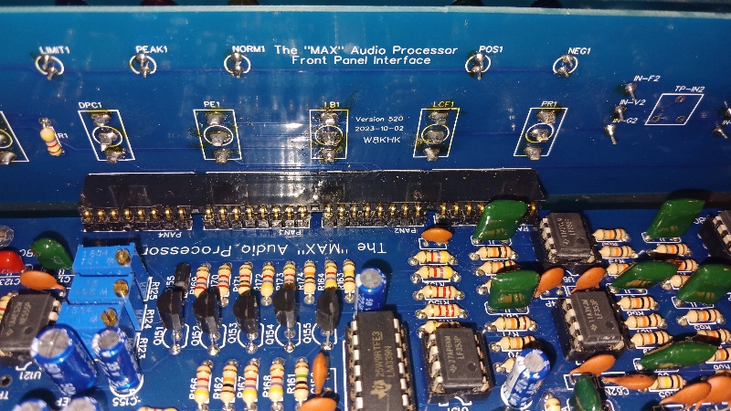
7: Front Panel
Assembly Procedure:
Earlier versions of the Max
Audio Processor (prior to revision level 500) require hand wiring of all front
panel LEDs, switches and potentiometers, a very tedious and error prone task at
best. Revision 500 introduced the “Front
Panel Interface” PC board, which provided direct connection to all the switches
and LEDs. Several prefabricated flat
ribbon cables are used to connect the interface board to the main board,
eliminating almost all the hand wiring.
Starting with 520 and later revisions, the individual flat ribbon cables
are replaced by a single 32-pin direct connection between the front panel
interface board and the main processor board.
The following sequence of steps must be followed to assure proper
alignment of all the components.
For revisions prior to 540: Prepare
the female Dupont receptacle for the Front Panel Interface to Main Processor
board connector as follows: Take a 40
pin Dupont female receptacle, and cut it at the center of pin 36, leaving 35
pins intact. Remove pins number 9, 18,
and 27 by pulling the protruding pin from the assembly until it is free. You will now have a connector with four
separate eight-pin groups, with one empty pin space between each group. For revisions 540 and later, install the full
40-pin connector as it is received in the kit.
This connector will be
mounted on the silkscreen legend side of the front panel interface board, and
it will be soldered on the side without the legends. When assembled, the connector and all
silkscreen legends will face the BACK of the processor, while all the
components will actually connect on the blank (non-silkscreen side of the
board. Solder one pin on each end of the
connector, verify perfectly accurate alignment, perpendicular with the board,
then solder one more pin in each group.
When satisfied that alignment is still perfect, solder the remaining
pins.
Front Panel Assembly Process Overview
1.
Attach the dress
panel securely on the 1U Rack panel or chassis front surface with clear tape.
2.
Mark hole
positions, sight the center location for each hole, and carefully center-punch
each location.
3.
Remove the dress
panel from the front panel or chassis.
4.
Drill a small
pilot hole at each centerpunch location, then enlarge each hole to the required
size.
5.
Temporarily
mount all switches on panel and dress panel, with only one nut at panel,
finger-tighten (loosely).
6.
Place Front
Panel Interface PC board on switches, with the silkscreen side to the back of
enclosure, solder switch terminals.
7.
Remove all nuts,
and remove switch and printed circuit board from panel(s).
8.
Insert all LED
wires into switch side of Front Panel Interface PC board, observing polarity,
then reattach assembly to front and dress panels.
9.
For desktop
enclosures, add a “back nut” and washer to each switch, and adjust such that,
when assembled, switch threads will have minimum reveal. No back nut is used for the 1U Rack
configuration.
10. Push each LED forward so that all LEDs protrude
evenly through the dress panel holes, and solder LED wires.
11. Remove assembly again, insert potentiometer leads
into Front Panel Interface PC board, and reassemble to front and dress panel. (Non-PC board style potentiometers will need
bare wires attached to connect potentiometer to the interface board.)
12. Secure each potentiometer with a nut, while
maintaining proper terminal pin alignment.
Solder potentiometer terminals to board.
13. Evenly tighten all switch and potentiometer nuts,
then install knobs on potentiometer shafts.
VERY
HELPFUL NOTE: While the standard SPDT
switches are typical standard ¼” mounting devices, most of the SPDT center off
switches likely use metric hardware, which is slightly larger. Ensure the hole for the bandwidth and density
switches are sufficiently large, AND keep the washer and nut hardware for the
switches separated, such that they are finally attached to the appropriate
switches.
Arranging
the switches on the front panel before soldering the front panel interface PC
board:

The assembly must be
completed within the desktop enclosure, however the preassembly of the panel
for the 1U rack may be accomplished with the aluminum panel separate from the
enclosure. In all cases, the initial
switch assembly step MUST be accomplished with the drilled aluminum front panel
and the glass epoxy silkscreened dress panel mated together.
When preparing the metal
back-panel, the holes in the LED locations should be slightly larger than the
LED holes in the dress panel, especially important if the back panel is of
thick material. This preparation will allow the LEDs to protrude, evenly,
through the dress panel holes, and all LEDs will have the same exposure when
installation is completed.
Soldering the switches to
the front panel interface PC board:
Please refer to the images
for additional detail while assembling the panel interface board
components. The board will be assembled
in stages, to assure alignment, and to enable the builder to handle the many
individual components to be interconnected. First the eight switches are
installed loosely on the back of the aluminum panel, with the dress panel
positioned in front of the aluminum panel. Only one nut, and no other hardware
should be used. They should be loose enough that the switches may rotate, but
not rock back and forth in the holes. There are SIX STANDARD SPDT switches, and
TWO SPDT switches with a CENTER-OFF POSITION. The two center-off switches must
be installed at the DENSITY and the BANDWIDTH locations on the right side of
the panel. ALL SWITCHES must have the locating key, or groove, facing the BOTTOM
of the panel BEFORE SOLDERING!
Next, view from several
angles to be sure the PCB is straight and even, not warped as it travels across
the array of switches. If all is well, slightly tighten the switches in the
dress panel to assure they are perfectly aligned, and solder the remaining
switch terminals.
The LEDs may now be
installed as follows. Remove the nuts on all eight switches and separate the
dress panel from the switch assembly.
After the switches are
soldered, LEDs and potentiometers may be added to the interface board:
Finally, the front panel
interface board is attached to the chassis and dress panel using the switch
nuts and potentiometer nuts.
With the thick 1U Rack
panel, no nut or washer will be placed on the switch behind the panel. the
front panel. For the desktop enclosure with the thin panel, it will be
necessary to place a nut and a washer on the switch before assembly. Determine
the proper location of the nut, such that when the front nut is tightened
against the dress panel and aluminum panel, no excess switch threads are
revealed in front of the nut. Then prepare all switches with the same
complement of nut and washer spacing items. The LEDs are inserted in the
connecting lands, from the switch side of the front panel printed circuit
board, with the positive (longer pin) UP, and the shorter pin matching the flat
side of the LED plastic housing DOWN. Insert them all the way, with the wires
protruding toward the silkscreen side of the board. You might wish to make a small bend at the
end of each LED lead to make sure they do not fall out of the interface board.
Attach the switch board to
the front panel, and securely fasten all eight nuts. Then push the LEDs
forward, such that each is inserted securely and evenly through the openings in
the front panel. Solder the LED wires, and clip the excess leads. You now have
a completed assembly that may be interconnected to the main board, and it may
also be easily disassembled if ever a component needs to be replaced.
If you have a front panel
with either two or four level control potentiometer locations, prepare the two
or four pots by adding short bare wires to the terminals, soldered such that
the wires protrude backwards about an inch or so. Bare wires left over from resistors or
electrolytic capacitors work well for this step. Remove the front panel circuit board from the
assembly, and then thread the pot leads through the three holes in the
interface PCB, but do not solder.
Reattach the front panel assembly to the front aluminum and dress
panels, with the pot shafts through the panel holes. Attach pot nuts, and tighten all pot and
switch nuts. Last, solder the pot wires
on the back of the interface board, and trim extra wire.
NOTE: If your board has a location for the switch
for Mid and Line input selection, install this switch at the same time you
install the pots. The power switch on
the right side may be installed at this point, and it might be easier to solder
lead wires to the switch before mounting it on the panel.
8: Processor Board
and Power Supply Integration
Mounting the Main Processor Board
Now that the front panel
assembly is completed, the main processor board connector may be inserted into
the front panel receptacle. Once properly
aligned, the location of the mounting holes for the main board may be
marked. While the main board has
mounting holes on all four corners, the back two holes are likely sufficient
support for the main board, but all four holes may be used if desired. At this point, locations for the
rectifier-filter board may be determined, and corresponding holes may be
drilled.
Four sets of conductive
stand-off mounts are provided for the main processor. Insulated stand-off mounts are provided for
the rectifier-filter board. Generic
hardware, also provided, may be used if an internal transformer option was
ordered. Finish mounting boards and
transformer, then continue with final wiring.
The power for the main processor board is provided by the rectifier-filter
board, via the flat four-wire ribbon cable provided. Polarity orientation is
not an issue with this cable.
Connecting an A.C. power supply:
The MAX processor circuit
includes a full-wave bridge rectifier and a series of regulators for both the
positive and negative busses. Builders have the option to either use a chassis
mounted transformer inside the cabinet or an external "wall wart"
supply with power brought in using an insulated barrel connector.
Some important information
regarding power transformers:
When choosing to use an
internal transformer, the builder is responsible for providing proper fusing,
power switch, input connector, and safely insulating all wires and terminals.
It is also critically important to use three wire power cords with the green
ground wire securely fastened to the chassis. The providers of the MAX Audio
Processor assume no liability for incorrectly installed or unsafe internal
power supply configurations. DO NOT choose to use an internal transformer unless
you are familiar with proper, safe installation requirements.
Internal Power Transformer Options:
If an external wall
transformer is used, no additional safety concerns exist. The only requirement
in this case is to make sure the wall transformer is connected to the MAX audio
processor via an insulated power connector. The AC lines entering the audio
enclosure must not be connected in any way to the metal enclosure or chassis.
This requirement is defined in order to avoid any ground loops that induce hum
or noise into the low-level audio circuitry.
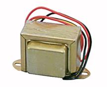
A chassis mount transformer
should either have a 24 VAC output with center tap (three leads 12-0-12) or two
12VAC secondary windings and be rated for 1 Amp or higher. For the first type,
the center tap is connected to power input terminal "AC_CT" on the
Rectifier/Filter board and the hot leads to power input terminals
"AC1" and "AC2". The dual secondary transformer would have
both secondaries connected at all four holes of "ACIN1" on the
Rectifier/Filter board , observing proper phasing of the two windings In this
case, the two center pins of the ACIN1 header are the "virtual"
center tap of the two 12 volt windings connected in series.
A chassis mount transformer should either have a 24 VAC
output with center tap (three leads 12-0-12) or two 12VAC secondary windings
and be rated for 1 Amp or higher. For the first type, the center tap is
connected to power input terminal "AC_CT" on the Rectifier/Filter
board and the hot leads to power input terminals "AC1" and
"AC2". The dual secondary transformer would have both secondaries
connected at all four holes of "ACIN1" on the Rectifier/Filter board, observing proper phasing of the two
windings. In this case, the two center pins of the ACIN1 header are the
"virtual" center tap of the two 12 volt windings connected in series.
|
Examples include:
|
|
|
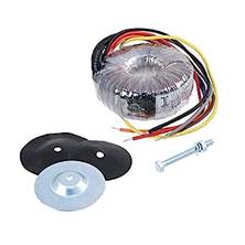
The toroidal transformer shown has two 12V secondaries
with all four leads connected to the Rectifier/Filter board at
"ACIN1". Examples include:
|
|
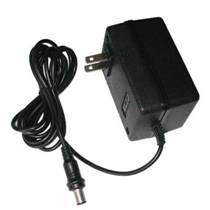
Wall Wart Option
|
A wall wart should have a 12 VAC output and be rated
for 1 Amp or higher. An insulated power connector must be used on the chassis
since both leads will be above ground potential. The two leads are connected
between power input terminals "AC1" and "AC_CT" on the
Rectifier/Filter board. Examples include: |
|
9: Audio
Interconnections
The MAX processor main board
should be securely grounded to the chassis or enclosure by either two, or
preferably four conductive stand-offs.
Therefor no ground wire is needed between the audio input or output
connectors and the main board. If the
mic input connecting wires are kept short, they need not be shielded. For long runs, shielding is recommended, and
the shield should be connected only at the processor board end, pin 1, and the
connector end of the shield should be left floating.
TRS ¼ inch connectors are
automatically grounded via their mounting hardware. XLR input connectors should be grounded by
running a short bare wire between the chassis ground pin and pin 1. XLR output connectors, when grounded, should
employ a cable from processor to transmitter, that is grounded only at the
transmitter end. This avoids unwanted
ground loops, as the processor is normally ground by the three-wire power cord. If a wall-wart power supply is used, then
either a separate substantial ground wire should be used to ground the
processor, or the ground may be satisfied by a contiguous ground on the XLR
cable between the processor and the transmitter. Eiter ground or leave the output XLR ground
pin floating, depending upon requirements for a proper ground connection, while
avoiding ground loops caused by multiple grounding paths.
For all input and output
connections on the processor, the positive signal is on pin 2, and the negative
is on pin 3 of the audio headers Mic, Line, Out1, and Out2. To complete the audio connections, wire the
positive pin 2 on the processor to pin 2 on the XLR connector, or the TIP pin
on the TRS connector. Wire negative pin
3 of the processor to pin 3 on the XLR connector, or to the RING pin on the TRS
connector.
10: Feature Options
and Jumper Settings
Extra Feature Settings:
The microphone input circuit
may be configured with a gain trim control (a 100 or 500 ohm trim pot at
location RG) or with a gain set jumper, by placing a 3 pin berg male jumper at
R16. With a jumper in the normal
position (R16 pin 2 and pin 3 connected) moderately high gain is provided,
appropriate for high quality balanced differential microphones intended for studio
or recording use. But if the jumper is
moved to connect pin 1 to 2, the microphone input preamp reverts to unity gain,
thus providing a second line input. This
is not accomplished by attenuation, followed by a high-gain preamplifier;
rather, it is implemented by reducing the gain of an already low noise, low
distortion input device, which exhibits exceptionally high rejection to
common-mode noise and hum.
The generation of the gain
reduction signal for the compressor may be configured to select either half or
full wave rectification. While most
processors manage gain reduction using both positive and negative content of
the input signal, a higher compression ratio, and therefore more dense
modulation envelope, may be accomplished if only the negative program content
is used to control gain reduction. This
is preferable for AM and sideband, but for FM it is critical that full wave
rectification is used to provide the most symmetrical output content. Half wave rectification is enabled by setting
LDR jumper to connect pin 1 to pin 2, while full wave rectification is enabled
by setting LDR to connect pin 2 to pin 3.
Positive peak limiting is
adjustable via trim pot R130. Initial
setting should be fully counterclockwise.
With this setting, the +100 / ASYM peak control switch has no effect; positive
peaks are limited to 100 percent, identical to the negative peak limiting. By adjusting trim pot R130 in the clockwise
direction, the bias on peak limiter transistor Q132 is increased, allowing
higher positive peaks only when the switch is in the ASYM (up) position.
Negative peak limiting, by
default, is set to 100 percent. Both
positive and negative peak limiting is of course dependent upon the proper
setting of the output level of the processor in concert with the modulation capability
of the transmitter. A single stage
negative peak limiter is, of course, not always perfect, and it is possible
that a rogue peak escapes the limiter, causing overshoot on rare
occasions. To deal with this situation,
a second stage negative peak limiter is available. In the unlikely event this
feature is needed, it may be adjusted by the bias setting pot R140. Initial setting of R140 should be maximum
clockwise, such that negative peaks are not unnecessarily restricted. Properly calibrated modulation monitoring equipment
is necessary for proper adjustment of this feature.
Required Jumper Settings:
There are several Berg
Jumper settings required for the operation of the processor. Some are used for diagnostics and
calibration, while others enable optional features.
Diagnostic and Calibration
Settings:
There are four diagnostic
test points available on the main processor board, labeled as follows:
1.
TP_B Compressor gain reduction bias signal (high
impedance, loading this test point will impact processing significantly)
2.
TP_C Processed signal, immediately following the
compressor
3.
TP_F Bandwidth control clock frequency (use 10K
resistor in series with scope or counter probe to avoid altering the frequency)
4.
TP_L Raw input level, pre-compressor
The compressor section may
be bypassed to provide a constant signal level to stages following the
compressor when making measurements, or when calibrating the bandwidth
filter. For normal operation, the
compressor section is enabled, but setting CMP jumper to connect pins 2 and
3. To disable the compressor, set CMP
jumper to connect pins 1 and 2.
The variable Bandwidth SCAF
filter may be disabled when testing the compressor or when performing frequency
and phase response tests, as it would naturally roll off the high frequency
response as the selected bandwidth frequency is approached. For normal operation, the SCAF section is
enabled by setting the jumper to connect SCAF pins 2 and 3. To disable and bypass the SCAF section, place
the jumper to connect SCAF pins 1 to pin 2.
The signal path between the
input preamplifier and the phase rotator provides a break point to insert an
internal EQ or other processing component at header EQ1. For normal operation, place a jumper on
header EQ1 from pin 6 (SND1) to pin 5 (RTN1).
The remaining pins on this header provide a ground reference and + and –
12 volt power to any desired internal accessory.
In order to support an
external EQ or other processor component via balanced differential connections,
the second balanced output circuit may be repurposed as a send source, and the
line input can be dedicated to a return input.
The jumper at three pin header INSRT is normally set to connect pin 1 to
pin 2, while the external insert function is enabled by setting the INSRT
jumper from pin 2 to pin 3. To operate
in this mode, the standard microphone input is used, selecting Mic input with
the Mic / Line switch bypasses the external EQ module, while selecting the Line
position passes the externally-processed program material on to the following
Max Processor modules.
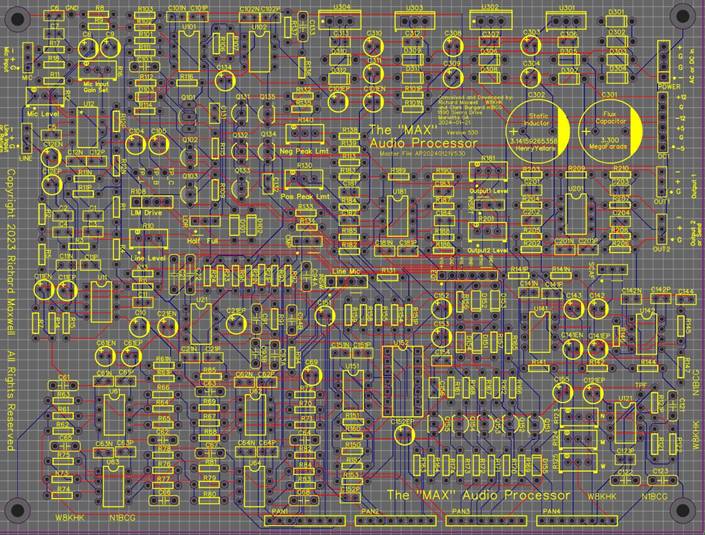
11: Illustrations –
Graphics and Photographs
The following illustrations
are presented below:
Main Processor board, 2D
view
Main Processor board, x-ray
view
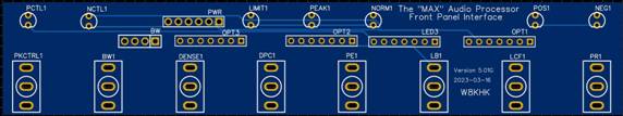
Front Panel LED, switch and
pot interface board, 1U rack version
Front Panel LED, switch and
pot interface board, mid-size desktop, style 1
Front Panel LED, switch and
pot interface board, mid-size desktop style 2
Front Panel LED, switch and
pot interface board, small desktop version
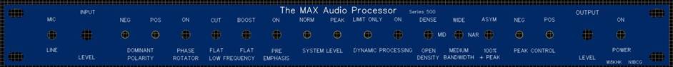
Front Dress Panel, 1U rack
version
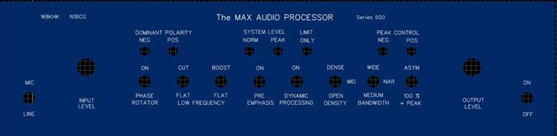
Front Dress Panel, mid-size
desktop, style 1
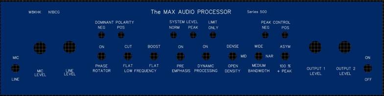
Front Dress Panel, mid-size
desktop style 2
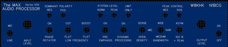
Front Dress Panel, small
desktop version
Rectifier Filter Printed
Circuit
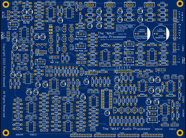
Main Processor board, 2D
view
Main Processor board, x-ray view
Front Panel LED, switch and pot interface board, 1U rack version

Front Panel LED, switch and
pot interface board, mid-size desktop, style 1
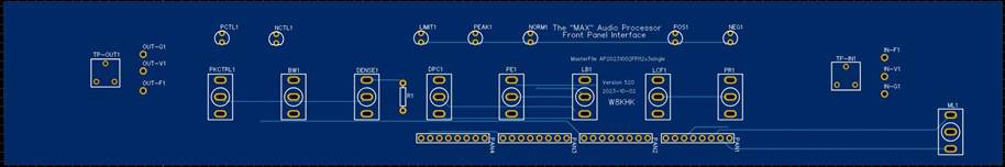
Front Panel LED, switch and
pot interface board, mid-size desktop style 2
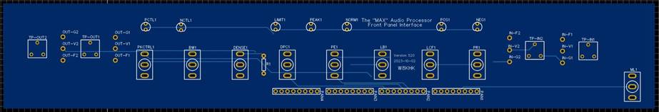
Front Panel LED, switch and
pot interface board, small desktop version
Front Dress Panel, 1U rack
version
Front Dress Panel, mid-size
desktop, style 1
Front Dress Panel, mid-size
desktop style 2
Front Dress Panel, small
desktop version
Rectifier Filter Printed Circuit